Apple Announces M3 SoC Family: M3, M3 Pro, and M3 Max Make Their Marks
by Ryan Smith on October 31, 2023 8:30 AM EST- Posted in
- CPUs
- Apple
- Arm
- Mobile
- SoCs
- N3
- Apple Silicon
- Apple M3
- Apple M3 Pro
- Apple M3 Max
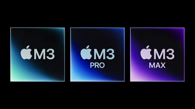
Capping off a busy month for new processor announcements, Apple this week has announced a new generation of M-series Apple Silicon processors – and with it, a newly refreshed generation of MacBook Pros. Anchored by the new M3 series of processors, Apple has opted to launch most of the stack in a single go, announcing products based on the vanilla M3, and more powerful M3 Pro and M3 Max SoCs at the same time. Built on TSMC’s N3B process, Apple is looking to once again raise the bar on both CPU and GPU performance, as well as setting a new record for the number of transistors used in a single laptop SoC.
The launch of the new M3 chips goes hand-in-hand with new MacBook Pro laptops, as well as a refreshed 24-inch iMac. But as Apple isn’t making any external design or feature changes to any of these devices – they’re all the same dimensions with the same ports and parts as before – they are a straightforward update to the internals of these devices. As a result, the star of the show for these latest product launches are the new M3 family of SoCs, and the features and performance they bring.
With their latest generation of high-performance silicon for Macs (and, undoubtedly, high-end iPads), Apple is seemingly taking full advantage of the density and power improvements offered by TSMC’s N3B process. But at the same time, they are also changing how their SoCs are configured; the M3 Pro in particular is a significant departure from its predecessor. So although the M3 chips do not in and of themselves rise to the level of “groundbreaking”, there are some important changes here that we’ll be taking a look at.
| Apple Silicon M3 SoCs | ||||
| SoC | M3 Max | M3 Pro | M3 | |
| CPU: Performance | 12-Core | 6-Core | 4-Core | |
| CPU: Efficiency | 4-Core | 6-Core | 4-Core | |
| GPU | 40-Core | 18-Core | 10-Core | |
| Display Controller | 5 Displays (1 Internal + 4 External) |
3 Displays (1 Internal + 2 External) |
2 Displays (1 Internal + 1 External) |
|
| Neural Engine | 16-Core 18 TOPS (FP16) |
|||
| Memory Controller |
LPDDR5-6400 32x 16-bit CH (512-bit) 400GB/sec Total Bandwidth (Unified) |
LPDDR5-6400 12x 16-bit CH (192-bit) 150GB/sec Total Bandwidth (Unified) |
LPDDR5-6400 8x 16-bit CH (128-bit) 100GB/sec Total Bandwidth (Unified) |
|
| Memory Capacity | 128GB | 36GB | 24GB | |
| Encode/ Decode |
8K H.264, H.265, ProRes, ProRes RAW, AV1 (Decode) |
|||
| USB | USB4/Thunderbolt 4 6x Ports? |
USB4/Thunderbolt 4 4x Ports? |
USB4/Thunderbolt 4 2x Ports |
|
| Transistors | 92 Billion | 37 Billion | 25 Billion | |
| Mfc. Process | TSMC N3B | |||
Starting things off, let’s take a look at the specifications for the three new M3 chips. With all three chips being released within a month’s time (technically the M3 Max devices don’t land until mid-November), this is the most ambitious launch yet of a new generation of M-series chips. Typically, Apple starts small and works their way up – e.g. M2 and then following with the Pro and Max variants farther down the line – but this time we’re getting what’s presumably all of the monolithic (and laptop-suitable) silicon parts in a single go.
But Apple is also starting smaller in terms of volume. The company is using these new chips for updates to the MacBook Pro lineup and an iMac, some of the company’s more expensive (and widely thought to be lower volume) products. This is in contrast to starting with the MacBook Air and other cheaper devices, which consume a much larger volume of entry-level chips. There’s a good chance that this is due to Apple’s decision to use a bleeding-edge node like N3B (a node they’re one of the only customers for), which would bring with it fresh chip yield and volume bottlenecks. But, of course, Apple will never confirm this. Either way, they’ve turned their chip launch strategy on its head for this generation by starting with more expensive devices first.
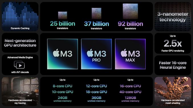
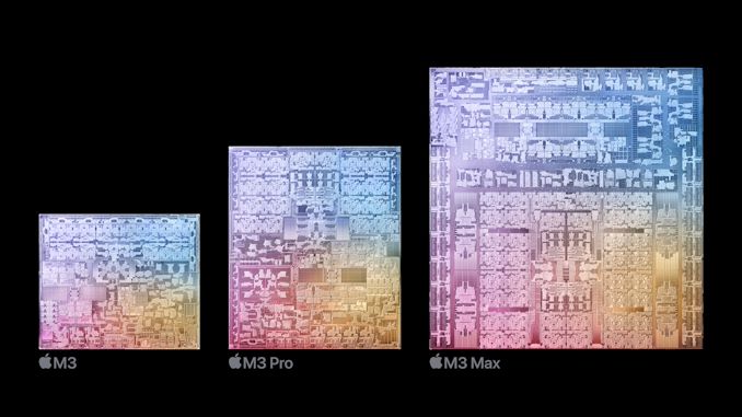
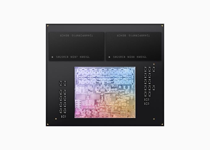
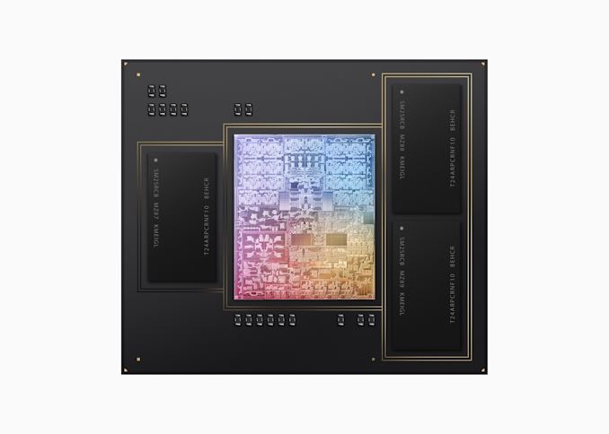
All three chips share a common architecture, and, broadly speaking, are scaled up versions of that architecture with more cores, more I/O, and a larger number of memory channels. The smallest chip, the M3, starts things off at 25 billion transistors (5B more than the M2), and things top out at the ridiculously stuffed M3 Max and its 92 billion transistors. While Apple supplies die photos (a true rarity in the industry these days), they do not supply die sizes, so we’ll have to see how these die sizes measure up once devices ship.
While Apple has not officially disclosed the process used besides it being a 3nm design, given that the only TSMC 3nm line that would have been available for this kind of high-volume production would have been their N3B line, it’s a very safe bet that we’re looking at N3B here, which was also used on the A17. According to TSMC official figures, N3B offers great transistor density, with a 42% reduction in feature size and a roughly 25% reduction in iso-power. But even so, the M3 Max is particular is still going to be a chonky chip.
Elsewhere, there doesn’t appear to be any changes to the types of memory Apple supports. The company’s bandwidth figures are, in a couple of cases, identical to the M2 series figures, indicating that the company is still using LPDDR5-6400 memory. This is a bit surprising to see, as faster LPDDR5X memory is readily available, and Apple’s GPU-heavy designs tend to benefit greatly from additional memory bandwidth. The big question at this point is whether this is because of technical limitations (e.g. Apple’s memory controllers don’t support LPDDR5X) or if Apple has made an intentional decision to stick with regular LPDDR5.
M3 CPU Architecture: Ambiguously Faster
On the architecture front, Apple is unfortunately being rather ambiguous about the CPU and GPU architectures used within the M3 family of SoCs. In fact, the company has kept a tighter grip on leaks there throughout the year – even now we don’t know the codenames of the CPU cores used in the A17 SoC.
In any case, given Apple’s shared use of CPU architecture between the A and M-series of chips, we’ve undoubtedly seen these CPU cores before. The question is whether we’re looking at the CPU cores from the recently launched A17 SoC, or the CPU cores from the A16 (Everest and Sawtooth). The A17 is the more likely candidate, especially since Apple already has working IP for N3B. But strictly speaking, we don’t have enough information to rule out the A16 CPU cores at this time; especially as Apple is not offering any guidance on the architectural improvements that the M3 family’s CPU cores offer over the M2.
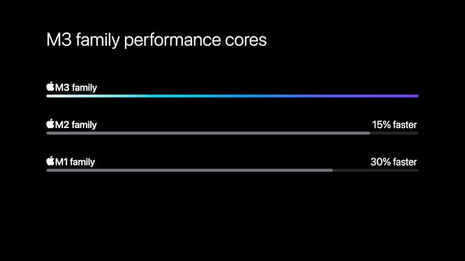
What we do know at this time is that, versus the M2 family, Apple is touting a roughly 15% improvement in the performance of its high-performance CPU cores. Or if you prefer an M1 comparison, a 30% improvement. Apple did not disclose the benchmark(s) or settings used to make this determination, so there’s not much we can say about how realistic that estimate is. Or, for that matter, how much of it comes from IPC uplift versus clockspeed uplift.
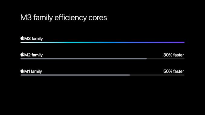
Meanwhile the efficiency cores have been improved upon as well, and according to Apple the gains are greater than with the high-performance cores. The M3 family efficiency cores are 30% faster than the M2’s, or a full 50% faster than the M1’s.
On their website, Apple has published application specific benchmarks, though these are system-level benchmarks. And many of which comingle CPU and GPU gains. Which are certainly going to be relevant to the users of those applications, but they don’t tell us much about the CPU cores themselves.
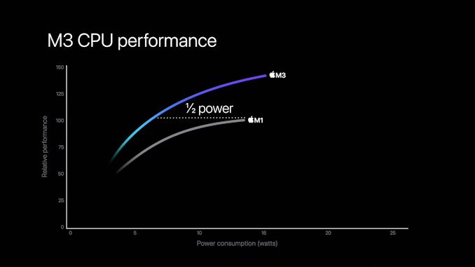
Apple’s equally nebulous performance/power curve graphs also largely reiterate these claims, while confirming that the long-term trend of perf/power curves getting flatter is holding. Case in point: Apple claims that the M3 can deliver the same CPU performance as the M1 at half the power; but peak-to-peak performance is only around 40% higher at iso-power.
Successive generations of process technology have continued to chip away at power usage from an iso-performance standpoint, but they’ve done relatively little to unlock higher clockspeeds. This makes continued performance gains from higher clockspeeds relatively expensive with regards to power, which in turn has pushed chip vendors to increase their power consumption overall. Even the M3 doesn’t escape this, as its peak power consumption is higher than the M1’s, according to Apple’s graph.
M3 GPU Architecture: A New Architecture with Mesh Shading & Ray Tracing
Meanwhile, on the GPU side of matters, the M3 family of chips packs a more substantial GPU architecture update. While Apple is as tight-lipped as always on the underlying organization of the GPU architecture, from a feature standpoint the new architecture is bringing some major new features to Apple’s platform: mesh shading and ray tracing.
These same features were also introduced with Apple’s A17 SoC for the iPhone 15 Pro family, and this is almost certainly a larger implementation of that architecture, as has been the case in prior generations. As we’re dealing with laptops and desktops here, these features would put the M3 GPU roughly on par with the latest discrete GPU designs from NVIDIA/AMD/Intel, all of whom have offered similar features for a couple of years now. In Windows parlance, the M3 GPU architecture would be a DirectX 12 Ultimate-class (feature level 12_2) design, making Apple the second vendor to ship such a high-feature integrated GPU within a laptop SoC.
At this point ray tracing needs little introduction, as the GPU/graphics industry as a whole has been promoting the far more physically accurate form of rendering heavily for the last half decade. Mesh shading, on the other hand, is less well known since it improves the efficiency of the rendering pipeline rather than unlocking new graphical effects. Its significance should not be underestimated, however; mesh shading upends the entire geometry rendering pipeline to allow for far more geometric detail at usable frame rates. It’s very much a “baseline” feature – developers need to design the core of their engines around it – so it won’t see much in the way of initial adoption, but it will eventually be a make-or-break feature that serves as the demarcation point for compatibility with pre-M3 GPUs. This is something we’re already seeing on the PC today with games such as the recently-released Alan Wake II.
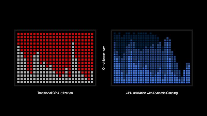
This GPU generation also comes with a new memory management feature/strategy, which Apple is dubbing “Dynamic Caching.” Based on the limited description within Apple’s product showcase, it appears the company has undertaken a new effort to better control and allocate the memory used by its iGPU, preventing it from allocating more memory than it actually needs. It’s common for GPUs to over allocate memory (better to have it and not need it than the inverse), but it’s wasteful, especially on a unified memory platform. As a result, as Apple puts it “only the exact amount of memory needed is used for each task,”
Notably, this feature is transparent to developers, and operates entirely on a hardware level. So whatever Apple is doing under the hood, it’s being abstracted away from developers and users alike. Though users will ultimately stand to benefit from more free RAM, which is unambiguously a good thing when Apple’s minimum configuration for an M3 Mac is still 8GB of RAM.
More curious, however, is Apple’s claims that this will also improve GPU performance. Specifically, that dynamic caching will “dramatically” improve the average utilization of the GPU. It’s not immediately clear how memory allocation and GPU utilization are related, unless Apple is targeting a corner-case where workloads were having to constantly swap to storage due to a lack of RAM. Either way, Apple considers this feature a cornerstone of the new GPU architecture, and it will warrant a closer look in the future.
With regards to performance, however, Apple is providing very little guidance. In past generations, the company at least provided a general compute throughput number for their GPUs, such as 5.6 TFLOPS for the vanilla M2 GPU. But for the M3 GPUs, we’re not getting any such throughput figures. So it is unclear, at best, how much faster these GPUs are in existing applications/games, or how much faster they could be. Apple is quoting a 2.5x figure on their product page, but checking the notes, this is Redshift with hardware RT (M3) versus software RT (everything else).
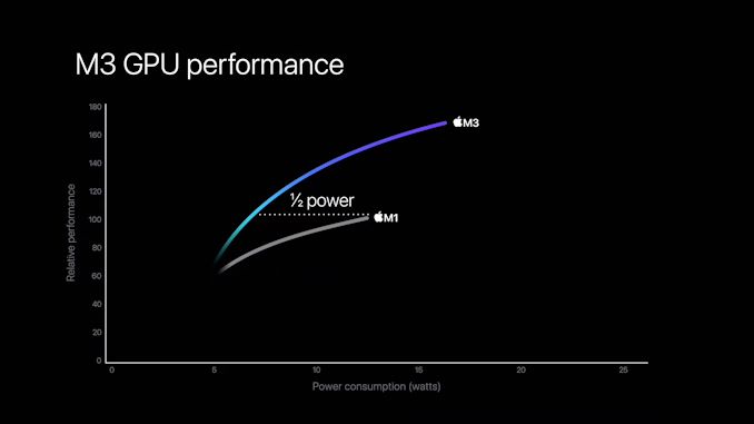
At best, Apple did show a GPU performance/power curve chart in their presentation, comparing the M3 to the M1. Apple again claims the M3 consumes half the power at iso-performance. Meanwhile performance at iso-power (peak M1, ~12.5W) is roughly 50% higher. But the M3’s GPU power limit is also significantly higher, reaching to about 17 Watts. Which unlocks further performance, but again consumes a fair bit more power – and doesn’t tell us how the M3 GPU compares to the M2.
M3 NPU: A Bit Faster, But Not Architecturally Updated?
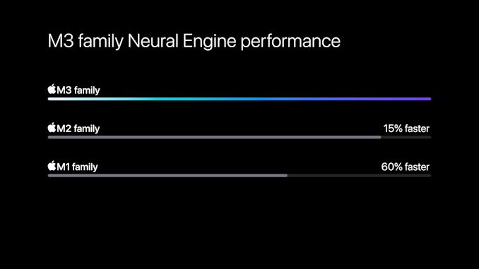
Last, but not least, let’s take a quick look at the M3’s NPU, the Neural Engine. At a high-level, this is once again a 16-core design. Apple claims that it offers 18 TOPS of performance, about 14% more than the M2’s NPU (Apple’s official figures have it at 15%, most likely due to dropping decimals). All three M3 chips seem to have the same 16-core NPU design, and thus should all have similar performance.
The 18 TOPS figure raises an eyebrow, however. As pointed out to me by former ATer (and potato enthusiast) Dr. Ian Cutress, 18 TOPS is actually slower than the NPU in the A17 SoC, which Apple quotes at 35 TOPS.
So what’s going on?
With the A17 SoC launch, Apple started quoting INT8 performance figures, versus what we believe to be INT16/FP16 figures for previous versions of the NPU (both for A-series and M-series). The lower precision of that format allows for it to be processed at a higher rate (trading precision for throughput), thus the higher quoted figure.
The 18 TOPS figure here is clearly INT16/FP16 performance, as that’s consistent with past M-series claims and Apple’s own chart. The question is leaves lingering, then, is whether the NPU in the M3 even supports INT8, given that it was just recently added for the A17. Either it does support INT8, in which case Apple is struggling with consistent messaging here, or it’s an older generation of the NPU architecture that lacks INT8 support.
The discrepancy is overall more of a curiosity than a concern. But it will be interesting to see if Apple has kept their NPU architectures for the A and M-series at parity, or if we’re seeing a divergence for this generation.
Just The Specs: M3 vs. M2 vs. M1
Getting back to speeds and feeds, I’ve also put together specification tables for each tier of M-series processors, comparing them to their immediate predecessors. This helps to better illustrate how these parts have evolved over time in terms of core counts, performance, memory support, and I/O.
| Apple M-Series (Vanilla) SoCs | ||||
| SoC | M3 | M2 | M1 | |
| CPU Performance | 4-core | 4-core (Avalanche) 16MB Shared L2 |
4-core (Firestorm) 12MB Shared L2 |
|
| CPU Efficiency | 4-core | 4-core (Blizzard) 4MB Shared L2 |
4-core (Icestorm) 4MB Shared L2 |
|
| GPU | 10-Core New Architecture - Mesh Shaders & Ray Tracing |
10-Core 3.6 TFLOPS |
8-Core 2.6 TFLOPS |
|
| Display Controller | 2 Displays (1 Internal + 1 External) |
2 Displays (1 Internal + 1 External) |
2 Displays (1 Internal + 1 External) |
|
| Neural Engine | 16-Core 18 TOPS |
16-Core 15.8 TOPS |
16-Core 11 TOPS |
|
| Memory Controller |
LPDDR5-6400 8x 16-bit CH 100GB/sec Total Bandwidth (Unified) |
LPDDR5-6400 8x 16-bit CH 100GB/sec Total Bandwidth (Unified) |
LPDDR4X-4266 8x 16-bit CH 68GB/sec Total Bandwidth (Unified) |
|
| Memory Capacity | 24GB | 24GB | 16GB | |
| Encode/ Decode |
8K H.264, H.265, ProRes, ProRes RAW, AV1 (Decode) |
8K H.264, H.265, ProRes, ProRes RAW |
4K H.264, H.265 |
|
| USB | USB4/Thunderbolt 4 2x Ports |
USB4/Thunderbolt 3 2x Ports |
USB4/Thunderbolt 3 2x Ports |
|
| Transistors | 25 Billion | 20 Billion | 16 Billion | |
| Mfc. Process | TSMC N3B | TSMC N5P | TSMC N5 | |
The vanilla line of M-series is the most straightforward of the family. The first of the M-series chips altogether, Apple has continued to grow the capabilities and the performance of the chip. But they have not added much in the way of functional blocks/cores. Three generations in now, and we’re still looking at 4P+4E CPU design, while the GPU has grown from 8 cores in the first generation to 10 cores in the M2 and M3.
Feeding the tiny beast has been a consistent 128-bit memory bus. With Apple not adopting LPDDR5X for this generation of the M-series, memory bandwidth remains unchanged from the M2, with up to 24GB of LPDDR5-6400 allowing for a 100GB/second of total memory bandwidth.
The limited I/O of the chip has also remained throughout the generations. The M3 can drive two 40Gbps USB4/Thunderbolt ports, the same as the M2 and M1. As well, there remains support for just two displays – the internal display, as well as a single external display.
Despite the lack of an increase in core counts, the transistor count has continued to grow over the generations, as new features and more complex core designs eat up larger transistor budgets. At 25 billion transistors, the M3 has 25% more transistors than the M2, or 56% more than the M1.
| Apple M-Series Pro SoCs | ||||
| SoC | M3 Pro | M2 Pro | M1 Pro | |
| CPU Performance | 6-core | 8-core (Avalanche) 32MB Shared L2 |
8-core (Firestorm) 24MB Shared L2 |
|
| CPU Efficiency | 6-core | 4-core (Blizzard) 4MB Shared L2 |
2-core (Icestorm) 4MB Shared L2 |
|
| GPU | 18-Core New Architecture - Mesh Shaders & Ray Tracing |
19-Core 6.8 TFLOPS |
16-Core 5.2 TFLOPS |
|
| Display Controller | 3 Displays (1 Internal + 2 External) |
3 Displays (1 Internal + 2 External) |
3 Displays (1 Internal + 2 External) |
|
| Neural Engine | 16-Core 18 TOPS |
16-Core 15.8 TOPS |
16-Core 11 TOPS |
|
| Memory Controller |
LPDDR5-6400 12x 16-bit CH (192-bit) 150GB/sec Total Bandwidth (Unified) |
LPDDR5-6400 16x 16-bit CH (256-bit) 200GB/sec Total Bandwidth (Unified) |
LPDDR5-6400 16x 16-bit CH (256-bit) 200GB/sec Total Bandwidth (Unified) |
|
| Memory Capacity | 36GB | 32GB | 32GB | |
| Encode/ Decode |
8K H.264, H.265, ProRes, ProRes RAW, AV1 (Decode) |
8K H.264, H.265, ProRes, ProRes RAW |
8K H.264, H.265, ProRes, ProRes RAW |
|
| USB | USB4/Thunderbolt 4 4x Ports? |
USB4/Thunderbolt 4 4x Ports |
USB4/Thunderbolt 4 2x Ports |
|
| Transistors | 37 Billion | 40 Billion | 33.7 Billion | |
| Mfc. Process | TSMC N3B | TSMC N5P | TSMC N5 | |
Things take a more interesting path with the M3 Pro, however. Unlike its siblings, which build upon their predecessors in a relatively straightforward fashion, for the third generation of M-series chips, Apple has rebalanced the M3 Pro. As a result, it has some significant differences from the M2 Pro in terms of configuration, and in terms of transistor count it has not been growing like the other chips.
Starting with the CPU cores, while the M3 Pro has 12 CPU cores in total like the M2 Pro, the balance between performance and efficiency cores has shifted. Specifically, it’s gone from an 8P + 4E design to a 6P + 6E design. And while all of the CPU cores in total are more performant than their M2 counterparts, this is why Apple’s official performance figures for the M2 Pro-equipped MacBook Pros show them only offering slim gains in CPU performance. For multithreading-heavy workloads, there really hasn’t been an increase in computational hardware.
The GPU core count has also slipped some, as well. The M3 architecture GPU offers 18 cores, versus the 19 found on the M2 Pro. This is as opposed to the vanilla M3 or M3 Max, which either held even or received a slight increase in GPU cores, respectively.
Finally, feeding all of this is a noticeably smaller memory bus. Both the M1 Pro and M2 Pro were equipped with a 256-bit LPDDR5 memory bus, which when populated with LPDDR5-6400, allowed for 200GB of aggregate memory bandwidth to the SoC. However on the M3 Pro, Apple has clearly cut the memory bus to 192-bits wide – removing a quarter of the memory bus – which in turn has decreased memory bandwidth by 25%, to 150GB/second.
The combination of these changes means that the M3 Pro, at a high level, looks more like a more powerful vanilla M3 than it does a cut-down M3 Max. Which, in some respects, is just a half-full/half-empty mindset. But overall, the balanced ratio of performance and efficiency CPU cores is much closer to the M3’s design, as is the total memory bandwidth. M3 Pro should still be noticeably faster than the M3, but in some areas it’s going to end up being a sidegrade from the M2 Pro in terms of performance.
Apple’s more conservative stance with the M3 Pro is also reflected in its transistor count. The number of transistors on the M3 Pro has actually gone down from the M2 generation – from 40 billion to 37 billion. So irrespective of the process node used, this is a slightly simpler chip overall. And compared to the M1 Pro, the transistor count has only marginally grown (~10%) over the previous two generations.
As for why Apple isn’t bulking up the M3 Pro like they have the other M3 SoCs, anything at this point would be a guess. But at a fundamental level, the M3 Pro should be meaningfully cheaper to produce than the M2 Pro, thanks to a combination of lower transistor count and smaller die size. N3B yields may play a part here (lower yields equal a higher effective cost for chips), but only TSMC and Apple know whether that’s truly the case.
Power consumption may also be a factor here, especially with the CPU core rebalance. 8 performance cores make for great performance, but they can certainly suck down a lot of power. The Max SoCs, to an extent, can get away with this because they’re top-tier chips that also go into high-end desktops and are otherwise aimed at desktop-replacement class laptop users. But for more mobile Mac users, Apple may be making a play to keep down power consumption by tamping down on performance growth.
For these reasons, it will be interesting to see how review benchmarks pan out. While this is unlikely to be a story Apple will ever tell, the performance and power consumption of their laptops should be able to tell a lot of the story for them.
| Apple M-Series Max SoCs | ||||
| SoC | M3 Max | M2 Max | M1 Max | |
| CPU Performance | 12-core | 8-core (Avalanche) 32MB Shared L2 |
8-core (Firestorm) 24MB Shared L2 |
|
| CPU Efficiency | 4-core | 4-core (Blizzard) 4MB Shared L2 |
2-core (Icestorm) 4MB Shared L2 |
|
| GPU | 40-Core New Architecture - Mesh Shaders & Ray Tracing |
38-Core 13.6 TFLOPS |
32-Core 10.4 TFLOPS |
|
| Display Controller | 5 Displays (1 Internal + 4 External) |
5 Displays (1 Internal + 4 External) |
5 Displays (1 Internal + 4 External) |
|
| Neural Engine | 16-Core 18 TOPS |
16-Core 15.8 TOPS |
16-Core 11 TOPS |
|
| Memory Controller |
LPDDR5-6400 32x 16-bit CH (256-bit) 400GB/sec Total Bandwidth (Unified) |
LPDDR5-6400 32x 16-bit CH (256-bit) 400GB/sec Total Bandwidth (Unified) |
LPDDR5-6400 32x 16-bit CH (256-bit) 400GB/sec Total Bandwidth (Unified) |
|
| Memory Capacity | 128GB | 96GB | 64GB | |
| Encode/ Decode |
8K H.264, H.265, ProRes, ProRes RAW, AV1 (Decode) |
8K H.264, H.265, ProRes, ProRes RAW |
8K H.264, H.265, ProRes, ProRes RAW |
|
| USB | USB4/Thunderbolt 4 6x Ports? |
USB4/Thunderbolt 4 6x Ports? |
USB4/Thunderbolt 4 4x Ports |
|
| Transistors | 92 Billion | 67 Billion | 57 Billion | |
| Mfc. Process | TSMC N3B | TSMC N5P | TSMC N5 | |
Finally, we have the biggest and badest of the monolithic M-series chip line, the Maxes. The Max chips have always pushed the envelope on core counts and transistor counts, and unlike the M3 Pro, the M3 Max continues this tradition.
Compared to its M2 predecessor, Apple has added another 4 performance CPU cores here, bringing it to a total of 12 performance cores and 4 efficiency cores. And making it the only M3 chip to get an increase in performance CPU cores. As a result, this will be the sole M3 chip that, at least in favorable thermal conditions, should see a significant increase in multithreaded CPU performance. Though “favorable thermal conditions” really is the operative word there, as this is a very powerful chip to cool.
On the GPU side of matters, the GPU core count has been increased slightly, going from 38 cores on the M2 Max to 40 cores on the M3 Max. Absent any good performance figures from Apple, it’s hard to estimate how much faster this will be in practice.
Feeding the M3 Max is the same 512-bit LPDDR5 memory bus as on the previous two editions of the chip. Notably, this means that Apple’s available memory bandwidth hasn’t increased over the past two generations to keep up with the larger number of CPU and GPU cores, so the company will need to be extracting more efficiency (and cache hits) from their chip architecture to keep the SoC well-fed.
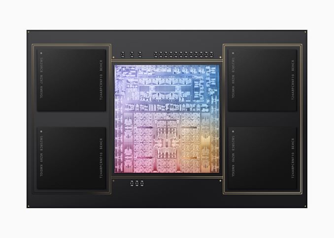
Looking at Apple’s official chip photo, we can see that Apple is once again using their bespoke x128 organization LPDDR5 memory chips, allowing them to have a 512-bit memory bus attached to just 4 chips. The maximum memory capacity in this generation has gone up to 128GB, which has interesting implications for the dies used within these memory chips. Unless Apple is doing something truly crazy, the only way to get 128GB of LPDDR5 would be to use 32Gbit LPDDR5 dies (32 in all). I’m not aware of anyone currently offering dies at that capacity, so it would seem Apple has secured first-dibs on that memory from whoever is offering it. For everyone else, we should see 128GB LPDDR5(X) configurations become available on Windows laptops later next year.
With the addition of CPU cores, GPU cores, and the general increase in the complexity of the various building blocks of the chip, the total transistor count of the M3 Max has ballooned to 92 billion transistors. This is 37% more transistors than the M2 Max, and 15% more (12 billion) than even NVIDIA’s massive GH100 server GPU, which is built on TSMC’s N4 process. The N3B-built M3 Max should be significantly smaller (under 400mm2?), but by laptop standards this is still a massive chip – never mind what happens if and when Apple puts two of them together for an Ultra configuration. However much Apple is paying TSMC for these chips, it can’t be cheap – but then how many other vendors are designing laptop SoCs with more transistors than most server chips?
M3 MacBook Pros: Coming Next Week
Wrapping things up, we’ll get to see Apple’s new M3 chips in action sooner than later. The company has already opened up pre-orders for the new MacBook Pro laptops, with the M3 and M3 Pro models expected to be delivered as soon as November 7th.
Meanwhile the M3 Max will be a bit farther behind, with Apple saying to expect them a bit later in November. Looking at the delivery estimates in Apple’s store, they shouldn’t be too far back – current delivery estimates have the laptops arriving by November 14th.
At this point Apple has retired all of their M2 Pro and M2 Max-based laptops – as well as the M2-based 13-inch MacBook Pro – so this looks to be a very quick transition on the laptop side of matters. Apple is still using the M2 Pro/Max chips in their desktop parts, such as the Mac Studio, but with all 3 M3 mono-dies already available, it’s only a matter of time until Apple gets around to upgrading their desktop line up as well.




55 Comments
View All Comments
Jansen - Tuesday, October 31, 2023 - link
It’s very possible this is built using N3E, especially at the relatively low volumes the MBP lineup has. The cost of N3B is also pretty high vs N3E, and I don’t see Apple rushing to adopt a high cost manufacturing process for the M3 series that won’t see 2025 as TSMC has already confirmed they will be moving past it.Don’t forget that the entire 3nm lineup from TSMC has been delayed, so Apple would’ve already been designing for a more mature 3nm process. Don’t have specifics on N3E mass production, but if it was July/August it could line up.
tipoo - Tuesday, October 31, 2023 - link
Well they also made some cuts especially on M3 Pro on core counts and down to a 192 bit memory bus, maybe to make up for the cost. They usually mention gen 2 3nm process or something telling but Apple-like vague like that.BillBear - Tuesday, October 31, 2023 - link
It's worth remembering that the top of the line Ryzen chips don't come anywhere near the M3 Pro's "reduced" memory bandwidth.TheinsanegamerN - Wednesday, November 1, 2023 - link
At 192 bit the m3 pro should be around 150GB/s.With new 8533 mhz memory AMD is pushing 137GB/s.
Apple's lead is disappearing.
BillBear - Wednesday, November 1, 2023 - link
With the Zen 4 Ryzen chips shipping now? No.AMD has about half the memory bandwidth of the M3 Pro.
valuearb - Thursday, November 2, 2023 - link
Max is still 400 Gb/s tho.repoman27 - Tuesday, October 31, 2023 - link
TSMC's first public statement about N3 timelines was during their Q1'20 earnings call, where they indicated that it would reach volume production in H2'22. TSMC eventually announced that milestone on December 29, 2022. N3 was not late.TSMC has always said that N3E would follow one year after N3, reaching volume production in H2'23. During their Q3'22 earnings call, C.C. Wei indicated that N3E might be pulled in 2 or 3 months, which would place it in the Sep-Oct 2023 timeframe. In their most recent earnings call on Oct 19, 2023, TSMC confirmed that N3E would reach volume production in Q4 of this year.
Ignore the media and analysts and pay attention to what TSMC is actually saying. The volume production milestone is a trigger for revenue recognition in subsequent quarters. TSMC is therefore very transparent about that, they have to be.
https://investor.tsmc.com/english/encrypt/files/en...
https://pr.tsmc.com/english/news/2986
https://investor.tsmc.com/english/encrypt/files/en...
https://investor.tsmc.com/english/encrypt/files/en...
my_wing - Wednesday, November 1, 2023 - link
TSMC is lier and will delete post. But old things do record itself in the internet.https://www.anandtech.com/show/16024/tsmc-details-...
The date the link headline is:
TSMC Details 3nm Process Technology: Full Node Scaling for 2H22 Volume Production
2H22 Volume Production and today we know is not is iPhone 14 on N3B node, Nope.
mandirabl - Tuesday, October 31, 2023 - link
I really like that they further diverged M3 Pro and M3 Max. Because they went all-in in M3 Max, which in turn will do wonders for the eventual M3 Ultra. Makes sense.TEAMSWITCHER - Tuesday, October 31, 2023 - link
I think people thought the M3 Pro would be the new vanilla M3. It will be very interesting to see the performance results. If the M3 Pro can beat the M2 Pro with fewer performance cores, then it bodes well for the entire M3 architecture as a whole.I would still love to see a deep dive into the core architecture details - instruction decoders, cores, and reorder buffers. Will Anandtech be able to figure any of this out, or will it require documentation from Apple?